This website uses cookies so that we can provide you with the best user experience possible. Cookie information is stored in your browser and performs functions such as recognising you when you return to our website and helping our team to understand which sections of the website you find most interesting and useful.
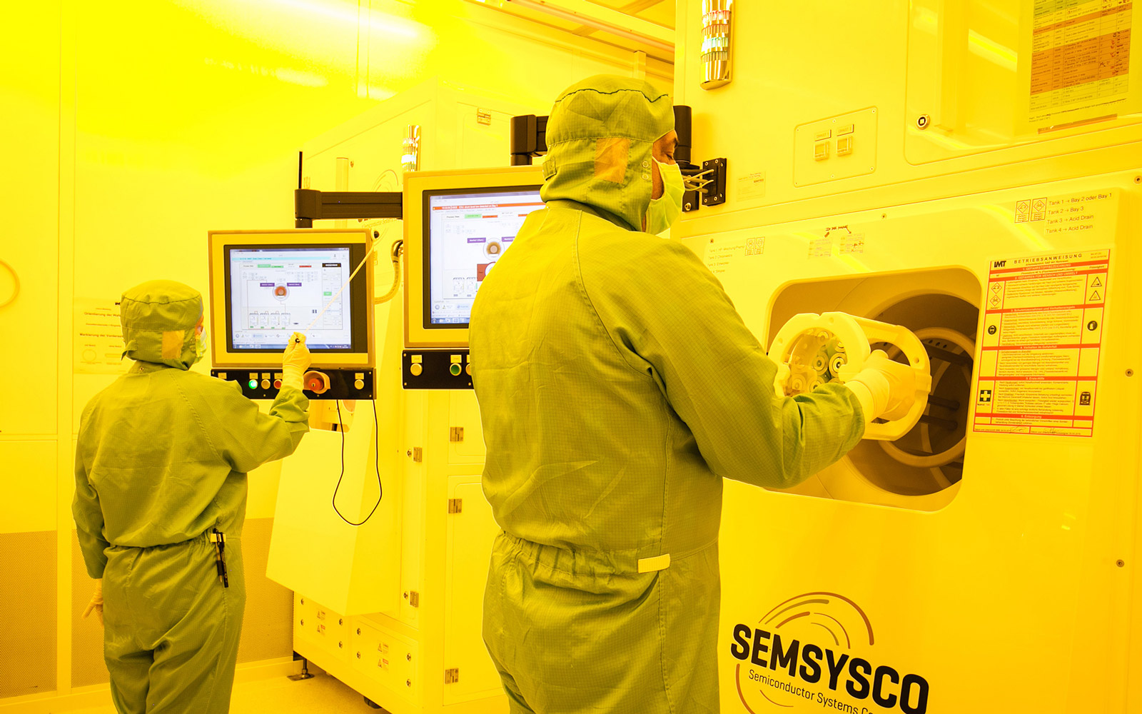
Etching technology
Etched: optical glass treated with hydrofluoric acid and RIE
In the clock and semiconductor industry, with MEMS and MOEMS, a wide range of etching processes, such as ‘Bosch’ (DRIE) and ‘LIGA’, has become firmly established. IMT differentiates fundamentally between two methods in glass processing:

Typical bath structure with HF
The image shows the characteristic topography of a wet-chemically etched channel. The edges are rounded and the ratio of channel width to channel depth is 2:1.

Wafer level capping for optical sensors
Depending on the application, optical senders and receivers must be hermetically sealed to protect them from environmental influences. In recent years, the TO housing has become firmly established at chip level.
Similar structures can be implemented very effectively at wafer level using etching processes. Wafers structured in this way are then bonded to the optical sensor wafer.
IMT produces 200-mm wafers in line with customer requests, which can then be further processed by the customer. The minimum wafer thickness is 0.3 mm.

Foturan 2 – photostructurable glass
Is it possible to achieve quick etching whilst maintaining the aspect ratio? With Foturan 2, Schott has developed a glass which does indeed meet this requirement. As a development partner of this Mainz-based company, we are delighted to be able to offer you this interesting option. As in standard lithography processes, the substrate is initially exposed.
The exposure defines a preferred direction for the etching process. In contrast to conventional processes, no photoresist is required for the exposure. The material’s properties make it extremely interesting for biotechnology and microfluidics:
- Chemical resistance allowing for biocompatible designs
- Low auto-fluorescence in comparison with plastic
- Temperature stability up to 400°C
- Option to autoclave and therefore reuse elements
- Excellent transmission in the visible spectrum