This website uses cookies so that we can provide you with the best user experience possible. Cookie information is stored in your browser and performs functions such as recognising you when you return to our website and helping our team to understand which sections of the website you find most interesting and useful.
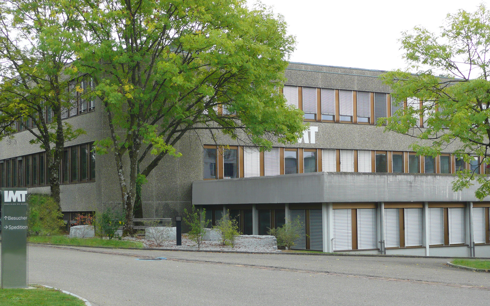
IMT – Precision on Glass
IMT has its roots in the microstructuring of metallic coatings on planar optical substrates. Over the years, we have continually added to this core expertise with complementary technologies.
Our solutions are now used in the semiconductor industry, medical technology, biophotonics, sports optics and optical measurement technology.
In addition to applications focussing on optical functions, the IMT product range also includes components with electronic and/or mechanical functions.
[accordion clicktoclose=”true” scroll=”true” tag=”h2″][accordion-item title=”Mission” id=”mission”]IMT is a leading global player in the development and production of customer-specific microstructures and thin films. Comprehensive services and innovative strength form the foundations of our long-term partnerships. With highly qualified employees and state-of-the-art technologies, we develop and produce key components and ensure constant progress and competitive advantages for our customers.[/accordion-item][accordion-item title=”Sustainability” id=”sustainability”]


 [/accordion-item][accordion-item title=”Milestones” id=”milestones”]
We take responsibility
IMT takes responsibility for people and the environment in all areas of the business. The way in which we think and act as a company is guided by sustainability. We meet the strictest statutory environmental requirements and ensure compliance with regulations through regular official inspections.
What’s more, we take additional measures which have a sustainable positive effect from both an ecological and economic perspective. For example, by introducing a special heat recovery plant, we have been able to reduce our power consumption by around 30% and heat consumption by around 80%, thereby making a contribution to reducing CO2 emissions.[/accordion-item][accordion-item title=”Memberships” id=”memberships”]
Many connections
IMT is a member of the following specialist associations and organisations:
2016
- Installation of bond cluster
- Installation of AOI
- Installation of the second HF etching system – 200-mm wafers
2015
- Installation of SEM – 200-mm wafers
- Installation of the bevelling machine
- Installation of the HF etching system – 200-mm wafers
2014
Final inspection becomes part of the clean room
2012
- Automatic sputtering system – 200-mm wafers
- Installation of the screen mask cleaner – 200-mm wafers
- Installation of the mask aligner – 200-mm wafers
- Installation of the HF etching system – 200-mm wafers
2008
Commissioning of the fifth CNC machine for glass machining
Increase of the share capital to CHF 12 million
2007
Introduction of RIE technology
2002
Opening of the branch office in the USA
2001
Commissioning of the first of three large evaporation systems for optical coatings
1999 – 2000
Complete renovation of the building infrastructure and conversion of production to manufacturing in clean room conditions
1995
Commissioning of the first direct write laser from industry pioneer Heidelberg Instruments for the production of large photomasks and optical calibration plates
1994
Integration into the HEIDENHAIN Group – subsidiary of Dr. Johannes Heidenhain GmbH, Germany
1968
Takeover by Mettler Instrumente AG, Switzerland – now Mettler Toledo
1959
Foundation by Dr E. Rüst under the company name Dr. Rüst AG