This website uses cookies so that we can provide you with the best user experience possible. Cookie information is stored in your browser and performs functions such as recognising you when you return to our website and helping our team to understand which sections of the website you find most interesting and useful.
Cleaning
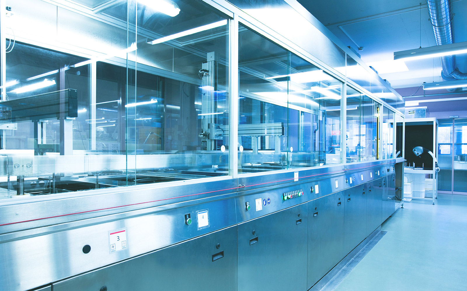
Cleanliness: clean processes require clean substrates
Cleaning is key when it comes to micro-optical and microfluidic elements. Clean raw substrates of a consistently high quality form the basis for reproducible production processes and high throughput. In comparison to macro-optical elements, such as lenses and mirrors, even the smallest contaminations or defects will lead to the failure of the end product. In this area too, IMT uses existing technologies from the semiconductor industry as well as a fully automatic cleaning line.

Screen Scrubber – Fully automatic cleaning machine for wafer cleaning
Wafer substrate: Fused silica, D263, Borofloat, Float, B270
Wafer format: ø 200 mm
Wafer thickness: 0.3 mm-4 mm
Throughput: 80 wafers/h
Cleaning technology: DI water mist, contactless brush cleaning on water film