This website uses cookies so that we can provide you with the best user experience possible. Cookie information is stored in your browser and performs functions such as recognising you when you return to our website and helping our team to understand which sections of the website you find most interesting and useful.
Semiconductor processes consistently implemented
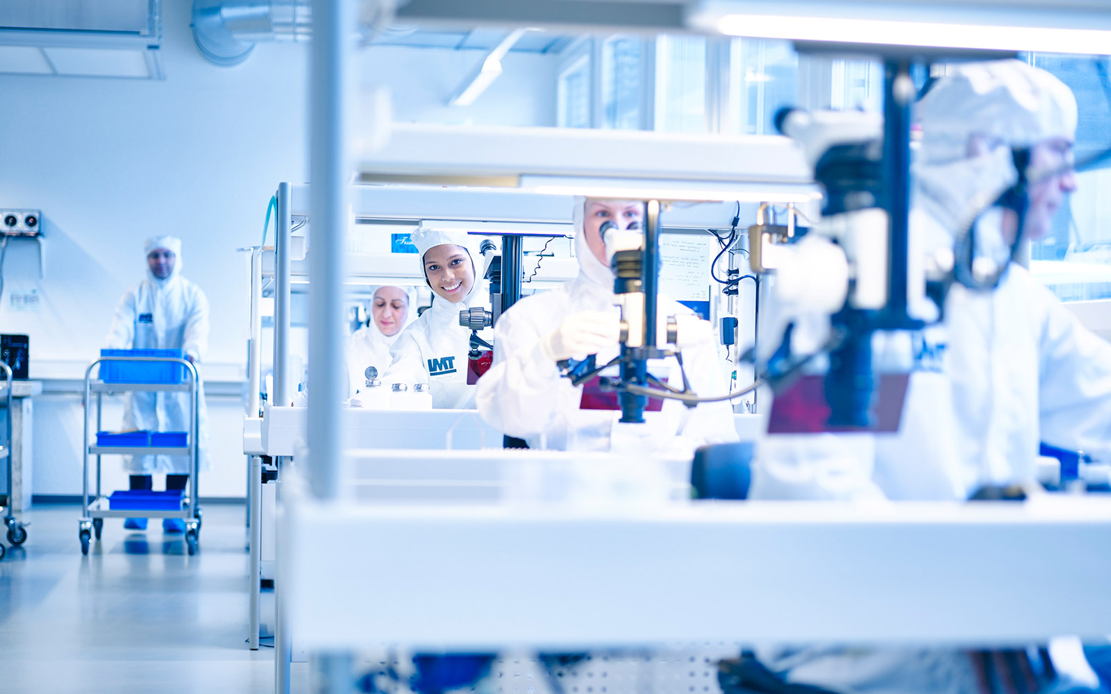
How do you produce cost-effective glass components of a consistently high quality with a high throughput? IMT answered this question at an early stage with the conversion to a 200-mm wafer line. Thanks to a future-oriented investment strategy, we now have equipment from the semiconductor industry along the entire value-added chain.
Our machinery
- Photoresist coating equipment for large formats up to 480 mm x 480 mm
- Laser plotters (DWL, direct write laser) for formats up to 800 mm x 600 mm
- Spin coater (200-mm wafers)
- Mask aligner (200-mm wafers)
- Plasma etching equipment (RIE, 200-mm wafers)
- Automatic HF etching systems (200-mm wafers)
- Wafer saws (200-mm-Wafer)
- Automatic wafer cleaner (200-mm wafers)
- Automatic optical inspection (200-mm wafers)
- SEM with EDX (200-mm wafers)
- Coating systems (PVD and sputtering)
- Interferometer
- Atomic force microscope (AFM)
- Confocal laser microscope