This website uses cookies so that we can provide you with the best user experience possible. Cookie information is stored in your browser and performs functions such as recognising you when you return to our website and helping our team to understand which sections of the website you find most interesting and useful.
Measurement technology
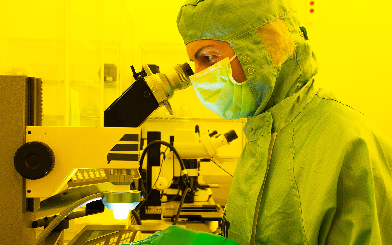
Measurement technology and process control make all the difference
The production of microsystems in the µ- and sub-µ range places incredibly high demands on the measurement technology used for process monitoring and final inspection.
Assessment and analysis of a wide range of structure sizes and shapes, in combination with a wealth of coatings, make the inspection processes extremely complex and the measuring tools used very costly.
As your reliable partner, IMT can provide you with elements which have been tested and inspected according to specifications.
The following measuring tools are used for measurement and analysis:
- Confocal microscope
- SEM (scanning electron microscope)
- AOI (automatic optical inspection)
- AFM (atomic force microscope)
- Tactile profilometer

SEM – where optical microscopes are stretched to their limits
Anyone producing nm structures should also be able to measure nm structures. On this basis, a scanning electron microscope was introduced in 2015. We are particularly proud of the fact that we are able to examine large substrates up to 200 mm in diameter. The system also has EDX (x-ray analysis) for the precise determination and analysis of foreign matter.

Automatic optical inspection
Automatic optical inspection is at the heart of numerous applications within the automotive and biotechnology sectors. The demand for top-quality, cost-effective elements in large quantities makes 100% inspection at 200-mm wafer level indispensable.
In this area too, IMT relies on proven technology from the semiconductor industry. In addition to the quick full measurement of the position accuracy and geometry of structures, it also allows us to detect surface defects down to a diameter of 2 µm.
The new system sets new quality standards and reflects our ongoing growth strategy.