This website uses cookies so that we can provide you with the best user experience possible. Cookie information is stored in your browser and performs functions such as recognising you when you return to our website and helping our team to understand which sections of the website you find most interesting and useful.
Machining
The finish: round, square or, if you would prefer, free form
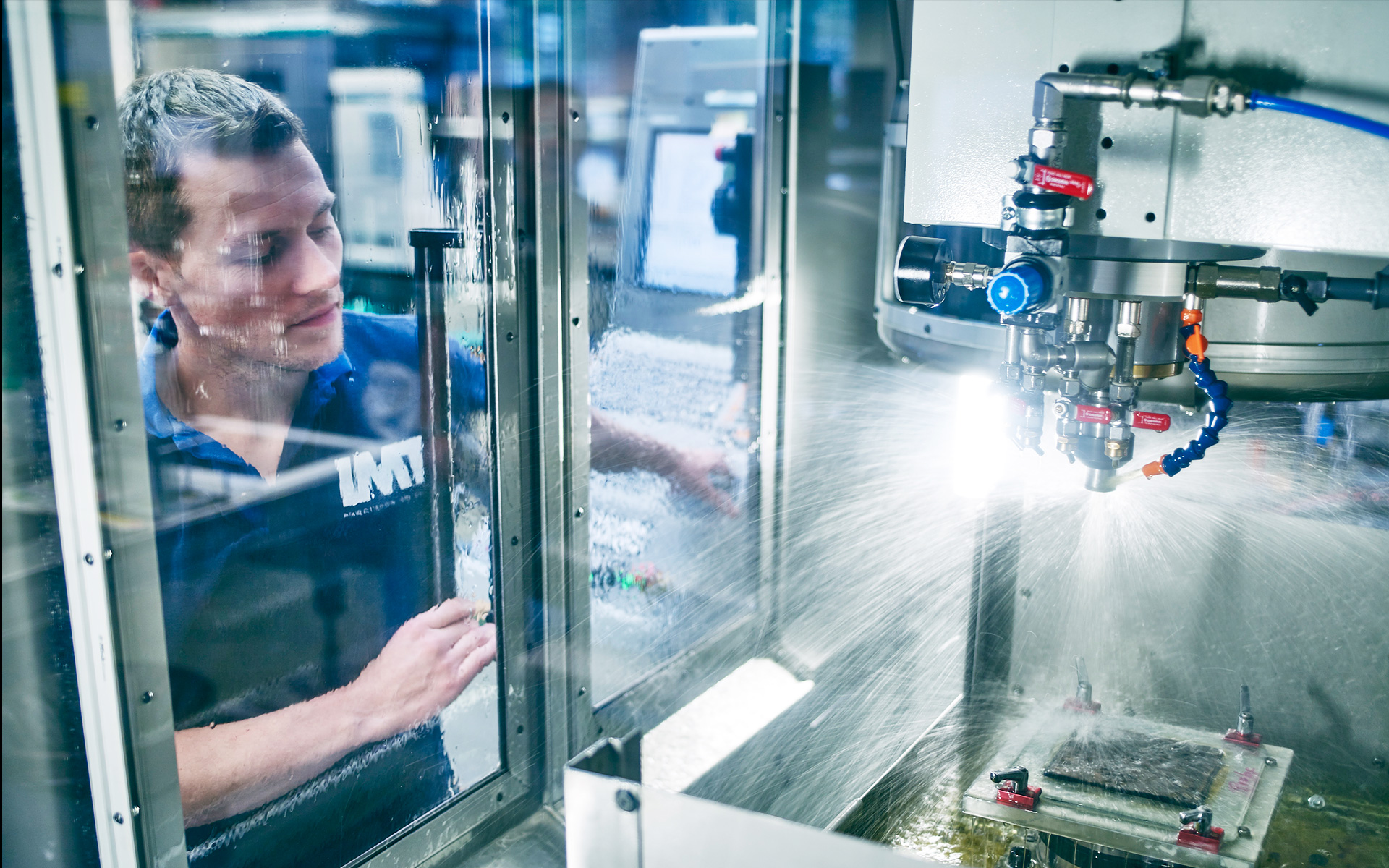
Machining, cleaning and inspection make up the end of the IMT process chain. In this area too, we offer a wide range of technologies and processes. In many applications a precise edge position in relation to the applied microstructure is important. As a result of continuous improvements, we are now able to achieve a level of accuracy from the sawn edge to the structure of < ±15 µm. In addition to numerous CNC machines, we use wafer saws from the semiconductor industry.

Wafer saw
Wafer saws are the default standard for sawing silicon chips within the semiconductor industry. Here at IMT, the same resources are used for the assembly of glass chips.
Substrate: all borosilicate glasses, not fused silica
Substrate thickness: ≥ 0.3 mm
Dimensions: ø ≤ 200 mm
Shape: square, rectangular
Edge breakouts: < 50 µm
Angle of the saw edge: 90° ± 0.5°