Biological applications drive feature aspect ratio and material selection

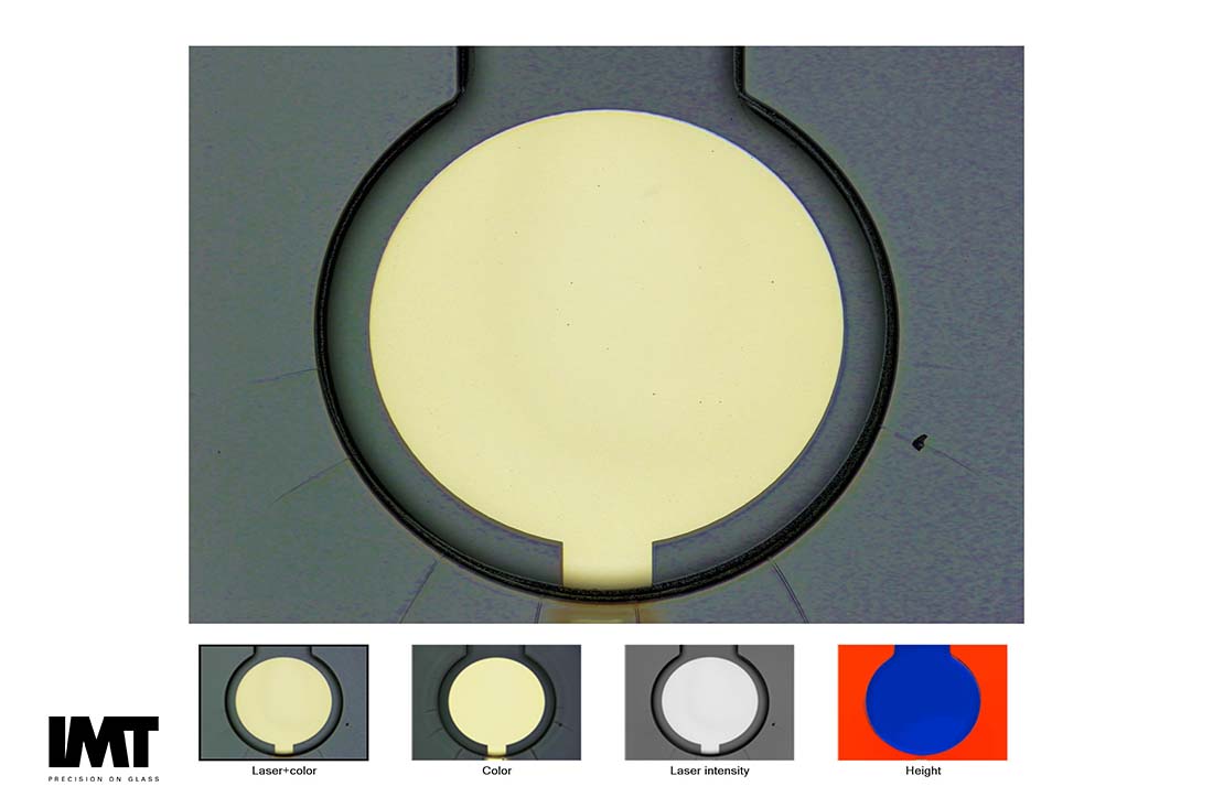
Au + SU-8 image. IMT provided prototypes of an electrical detection system of SNPs. Lithographically structured Au-electrodes on a D263 T ECO wafer of Schott. Capture and measurement cavities structured in a 350 micron thick SU-8 layer with an aspect ratio of 1:1.
Though using materials such as polydimethylsiloxane (PDMS) with soft-lithography is often the first and only step of a well-established manufacturing road-map for academic research, glass has many advantages to these materials, largely due to its mechanical, chemical, and optical properties [1, 2]. For example, for nano or microchannels, wall rigidity and stability become important, particularly if it is to survive the bonding or sealing process. Additionally, as dimensions shrink to the “extended nanospace,” the superior ability of bonded glass to withstand high pressures from fluid flow becomes a significant driver for glass material as the material of choice [3].
High aspect ratio channels are often required for biological applications. For example, high aspect ratio features are used to confine a single cell or create a specific flow profile. In many cases, silicon is the best material choice for high aspect ratio features, with the processing methods for silicon offering the possibility of arbitrarily high aspect ratios [4].

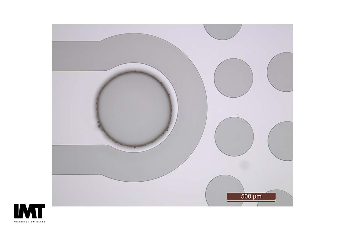
Lithographically structured 30µm thick SU-8 structured bonded by thermo-compression between two D263 T ECO wafer of Schott with fluidic access holes. [IMT]
However, applications for drug discovery, synthesis, DNA sequencing and PCR may require high aspect ratios coupled to other specifications. For example, assays and diagnostics may require the thermal properties of glass, as well as its stability to chemicals, and optical transparency by negligible auto-fluorescence. Finally, the glass surface is infinitely tunable by adding silanization reactions, allowing device developers to imbue the surface with specific properties utilizing standardized CVD processes.
When the specific glass material features (e.g. optical smoothness, dielectric constant, metal layer processing step requirements, bonding methods etc.) are desired, their combination with high aspect rations is achieved by a process that combines laser micromachining and chemical etching, aspect ratios as high as 20:1 have been demonstrated by Bellouard, et al., in glass [5].
Fused silica wafer processing offers a path to create microchannels and nanochannels with high aspect ratios using existing methods for fabricating optical gratings and other optical features in glass.

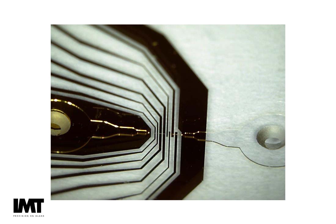
Lithographically produced Au-electrodes on a D263 T ECO wafer of Schott. Intermediary layer of TMMF defining the channels was bonded by thermo-compression on a second wafer with electrical and fluidic access holes.
Impedance-based microfluidic sensors measure the dielectric properties of particles, for example, cells, blood cells, or circulating tumor cells flowing in a channel with integrated electrodes. Usually, there are two electrode configurations, i.e. co-planar electrodes and opposing electrodes as in the image above. A co-planar configuration generates a non-uniform electric field, thus leading to a significant variation in signal strength for identical particles. In contrast, the opposing electrode configuration provides a homogenous electric field and enables a better detection and discrimination of the particles [6, 7].
Fabricating opposing electrodes is challenging due to the difficulty of patterning electrodes inside isotropically etched microchannels due to process constraint of standard microlithographic processes. In order to complete a microfluidic EIS sensor one would require a third layer that is to define the channels and is bonded between the two wafers with electrodes as well as fluidic and electric access holes. Here photo-structurable dry photoresists offer an alternative. TMMF dry photopolymer has been demonstrated to be a good alternative [7]. This material offers a combination of properties such as non-cytotoxicity, capability of tenting over deep trenches as well as high thickness uniformity that make it attractive for numerous BioMEMS applications [8]. With a wide variety of applicable dry photoresist materials, this is an attractive solution [9].
Recently new possibilities in glass processing have been added to the process portfolio by combining advances in laser processing utilizing ultra-short pulsed laser technology and wet etching techniques [10] [11] [12] [13]. This combined technology has been already is commercially available through several companies including by FEMTOprint of Switzerland [14], LightFab of Germany, [15] or LPKF for an efficient way of producing through holes [16].
Works Cited
[1] C. Iiescu, H. Taylor, M. Avram, J. Miao and S. Franssila, "A practical guide for the fabrication of microfluidic devices using glass and silicon.," Biomicrofluidics, vol. 6, no. 1, pp. 016505-016505-16, 2012.
[2] K. Ren, J. Zhou and H. Wu, "Materials for Microfluidic Chip Fabrication," Accounts of Chemical Research, vol. 46, no. 11, pp. 2396-2406, 2013.
[3] L. Mou and X. Jiang, "Materials for Microfluidic Immunoassays: A Review," Advanced Healthcare Materials, vol. 2017 Mar 21. doi: 10.1002/adhm.201601403. [Epub ahead of print], 2017.
[4] N. R. Glass, R. Tjeung, P. Chan, L. Y. Yeo and J. R. Friend, "Organosilane deposition for microfluidic applications," Biomicrofluidics, vol. 5, no. 036501, 2011.
[5] Y. Bellouard, A. Said, M. Dugan and P. Bado, "Fabrication of high-aspect ratio, micro-fluidic channels and tunnels using femtosecond laser pulses and chemical etching," Opt. Express , vol. 12, pp. 2120-2129, 2004.
[6] K. Kalkandjiev, A. Yusof, J. Schondube, R. Zengerle and P. Koltay, "Wafer-Level Fabrication of Microfluidic Sensors for Impedance Spectroscopy with Integrated Opposing Electrodes," 2011. [Online]. Available: http://www.imtek.de/data/lehrstuehle/app/dokumente/conferences-pdf/conferences-2011/kalkandjiev-wafer-level-fabrication.pdf.
[7] K. Kalkandjiev, L. Riegger, D. Kosse, M. Welsche, L. Gutzweiler, R. Zengerle and P. Koltay, "Microfluidics in silicon/polymer technology as a cost-efficient alternative to silicon/glass," J. Micromech. Microeng., vol. 21, p. 025008, 2011.
[8] S. Halldorsson, E. Lucumi, R. Gomez-Sjoberg and R. M. Fleming, "Advantages and challenges of microfluidic cell culture in polydimethylsiloxane devices," Biosensors and Bioelectronics 63 (2015) 218–231, vol. 63, pp. 218-231, 2015.
[9] P. Vulto, N. Glade, L. Altomare, J. Bablet, L. Tin, G. Medoro, I. Chartier, N. Manaresi, M. Tartagni and R. Guerrieri, "Microfluidic channel fabrication in dry film resist for production and prototyping of hybrid chips," Lab Chip, vol. 5, no. 2, pp. 158-62, 2005.
[10] L. Jonusauskas, T. Tickunas, A. Narmontas, G. Nemickas, V. Purlys, G. Grigaleviciute and R. Gadonas, "Femtosecond laser-assisted etching: making arbitrary shaped 3D glass micro-structures," Proc. SPIE 10520, Laser-based Micro- and Nanoprocessing XII, vol. 105201G, no. doi: 10.1117/12.228690, p. https://doi.org/10.1117/12.2286906, 2018.
[11] M. Hermans, J. Gottmann and F. Riedel, "Selective, Laser-Induced Etching of Fused Silica at High Scan-Speeds Using KOH," JLMN, vol. 9, no. 2, pp. 126 - 131., 2014.
[12] M. Yonemura, S. Kato, K. Hasegawa and H. Takahashi, "Formation of Through Holes in Glass Substrates by Laser-Assisted Etching," JMLN, vol. 11, no. 2, pp. 143-146, 2016.
[13] D. Wu, S.-Z. Wu, J. Xu, L.-G. Niu, K. Midorikawa and K. Sugioka, "Hybrid femtosecond laser microfabrication to achieve true 3D glass/polymer composite biochips with multiscale features and high performance: the concept of ship-in-a-bottle biochip," Laser Photonics Rev., vol. 8, no. 3, pp. 458 - 467, 2014.
[14] FEMTOprint, "3D micro-fluidic channels," 2015. [Online]. Available: https://docs.wixstatic.com/ugd/fa0c43_8a466e7497424beab5fe25cfbde96315.pdf.
[15] LightFab, "SLE: Selective Laser-induced Etching (also known as ISLE: In-volume SLE)," 2018. [Online]. Available: https://www.lightfab.de/index.php/SLE-Technology.htm.
[16] LPKF, "LIDE - Laser Induced Deep Etching," [Online]. Available: http://www.lpkf.com/applications/lide-technology/index.htm.

